Features:
1. The shell feeding component adopts an HTCC high-temperature ceramic design structure, effectively increasing lead density and airtightness reliability, and meeting the miniaturization requirements of packaging modules. In special requirements, glass melt sealed feedthrough structures can also be used.
2. The bottom plate of the shell heat dissipation is generally made of tungsten copper and molybdenum copper materials, with a maximum thermal conductivity of 260W/m.K.
3. The coating of the shell can be adjusted according to the characteristics of the user's micro assembly process, which can meet the welding processes of lead tin, gold tin, gold germanium, and different atmosphere conditions.
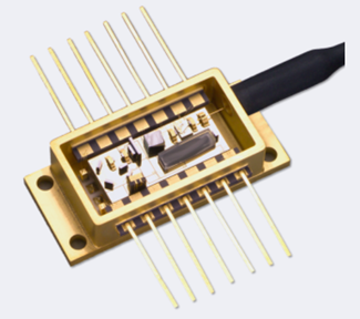
The company currently produces 3 types butterfly shaped packaging shells and can customize them professionally according to customer needs
working principle:
The working principle of a butterfly laser is to use the PN junction of semiconductor materials and an external electric field to achieve electro-optical modulation (LD chip). When the applied voltage increases, electrons and holes will aggregate in the PN junction, forming charge carriers, thereby changing the recombination rate and lifetime of charge carriers. This can generate dispersion and absorption effects to adjust the phase and intensity of light, thereby achieving electro-optic modulation.
Specifically, when a voltage is applied to the modulator, electron hole pairs form dominant charge carriers and form another layer of refractive index variation region in the waveguide region, which is used to change the refractive index in the waveguide. In this way, the refractive index change in the waveguide can be adjusted by the density of charge carriers, thereby achieving phase modulation. In addition, the PN junction set in the modulator region can be used to change absorption and transmission, thereby achieving intensity modulation.
 English


